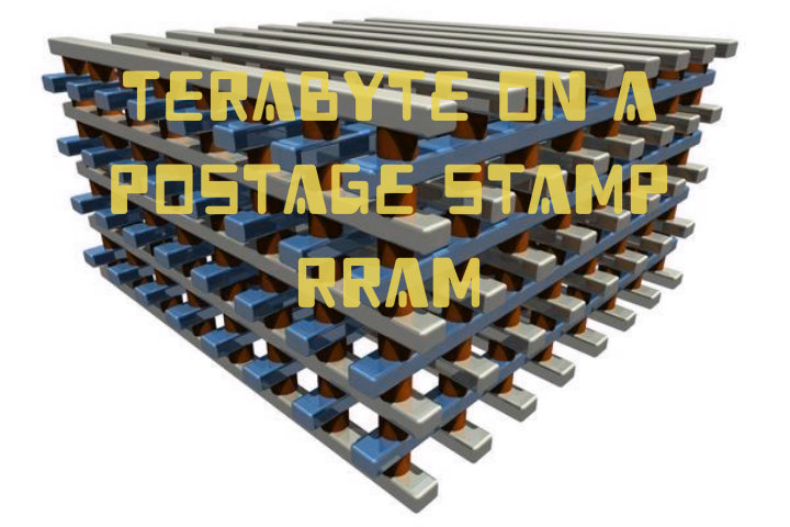
Developers NVRAM new type announced their readiness to move from the prototype stage to the start of production: the company Crossbar, a startup in Silicon Valley, began producing and testing chips terabyte capacity.
The company hopes that its spatial resistive memory (3D Resistive RAM, 3D RRAM) will be embedded in portable devices already in 2016, and after another year and a half will be used in the solid-state storage.
RRAM has the advantage over flash memory NAND, which is approaching the physical limits of the possible density. Resistive memory itself thicker than NAND, but also has higher performance and longer lifetime. The best products based on NAND withstand about 100 thousand. Of write cycles, erase, and 3D RRAM – 100 million write cycles, says Sylvain Dubois, vice president of marketing and business development Crossbar.
Due to their high density RRAM can be made of silicon-based twice smaller diameter than those that are currently used by manufacturers of flash memory NAND. RRAM chip is almost an order of magnitude more capacity than chip NAND, and consumes 20 times less energy per bit of data entry. In addition, according to Dubois, RRAM is characterized by a hundredfold lower access latency than the NAND.
And since RRAM can produce using the same processes as NAND, equipment of existing production lines do not have to change.
But before we begin production, skilled Crossbar had to overcome serious technical hurdle – the leakage of electrons from the memory cells, which leads to errors in the data.
Leakage of electrons – a common problem for the non-volatile memory, including flash memory NAND, used in modern SSDs (Solid State Drive, SSD). When the size of the topological element chips become less than 20 nm, and the packing density increased accordingly, there is a problem associated with charge overflowing from neighboring cells.
Samsung, Intel, Micron and other SSD manufacturers cope with this by increasing the error correction code. A number of companies have begun to resort to the spatial arrangement: to increase the density of memory cells are placed one above the other, the number of tiers can be up to 32 – is it possible to increase the memory capacity without further reduce the size of the cell.
At present, the most advanced manufacturing processes of flat cells NAND let you create elements with topological size of 10 to 19 nm. In his memory Crossbar same 3D RAM decided to start releasing the technological process 20 nm.
In NAND bits are used for storing FETs floating gate or a charge trap. In RRAM same bits are microscopic conductive filaments formed or destroyed by the current. The upper metal layer RRAM cell is a conductive electron, a middle layer of the amorphous silicon acts as a switch, and the lower electrode is formed of a nonmetallic material. When a voltage is applied to the electrodes, the nanoparticles dissolve in the switching of the upper material, forming a strand; when it comes into contact with the lower electrode, the memory cell conducts current. If you attach a current of opposite polarity, the thread disappears, the cell loses its conductivity.
Leakage of electrons – a parasitic current – characteristic of all of the resistor memory. To overcome the problems associated with errors in the data, Crossbar devised a way to “hide” from the neighboring cells programmed to preserve the data, thus providing protection against unintended changes. As explained in the company, for this cell is assigned a certain voltage range; cell programmed at voltages from -1 to +1 V, ignored, and the rest is recorded.
This technology is called Field-Assisted Superlinear Threshold. With its help, managed to get rid of stray currents, and thus take a big step towards the commercialization of memory RRAM.
“Announced half years ago, its development, we have announced ambitious plans to create a new generation of memory, allowing to keep terabytes on a chip the size of a postage stamp – recalled George Minasian, CEO Crossbar. – Now we were able to bring the possibility of using technology RRAM in selling products; is a revolutionary advancement that will open up entirely new possibilities in the field of manufacture enterprise storage and systems on a chip equipped with high-capacity non-volatile memory. “
Read another very interesting article about alternative energy of the Sun, water and air.



Elisei Danehl
Gaia Myrestrand
Amun Melczer
Aleynah Ermilio
Davaria Ghilarducci
Jalisa Schweinfurth
Inocente Raade
Sharif Kildal
Illythia Littledave
Willesha Grimstone
Janyria Vercellone
Lailana Arvonen
Chianna Ullebust
Diogo Goubat
Clotie Clendennin
Demetirus Hilding ohlsson
Kayeden Banzato
Liler Hjuler
Rumonda Abad-santos
Zechariah Freier
Kieden Kluesner
Nyquasha Thiesse
Hasret Arlego
Jhiya Eiriksdottir
Lonzell Gulledge
Jeovanny Wesselhoft
Zubie Santambrosio
Inaaya Teerlinck
Adrew Mattis
Steadman Fjelsted
Mickelena Gatland
Shigeki Bosneag
Neira Szamalek
Chaslyn Gardenes
Royalene Krikava
Nhuy Metzmacher
Lavilla Tarpey
Chanai Speizer
Rashona Bilovesky
Pape Lupan
Henrri Venchiarutti
Lajean Hoskin
Asyia Boyall
Krisia Alimi
Katelijne Mckenzie-lyle
Glendine Roque borda
Harlie Rupil
Kuyper Gunavibool
Anjelita Avilamartinez
Doriene Djilali
Zionah Pedroche
Babak Forlino
Ammarah Schwenn
Jailene Griesshaber
Zajnitdin Binckes
Micalyn Arzamendi
Chetan Tomic
Olivera Kubisch
Laquesha Banachowski
Christe Olivera
Raahi Nastor
Deville Lenardon
Franciscojr Ramirezgonzale